
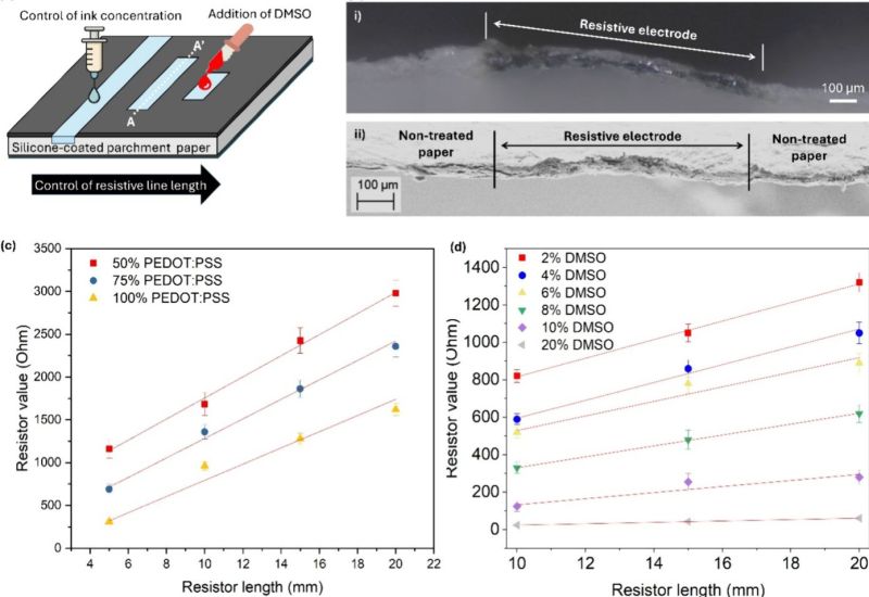
The nice thing about the inks used with papertronics that they aren’t just traces, but can also be functional elements like resistors, which is also demonstrated in the paper. The channels for the inks are created using a 50 Watt CO2 laser, which etches away the silicone coating on the parchment paper. The achieved resolution in the article is around 250 µm for line widths and 300 µm line spacing, which is much better than that for wax-based alternatives.
Providing conductivity in the inks was PEDOT
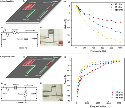
 SS, which, when mixed with dimethyl sulfoxide (DMSO), creates resistors. Capacitors can be printed by creating interlocking PEDOTSS ‘fingers’, with a Poly Vinyl Alcohol (PVA) based gel overlaid as electrolyte. These combinations were used to create RC low- and high-pass filters.
The degradation of these papertronic circuits was also tested, with them buried in soil under typical conditions. Only the silicone coating was rather immune to degradation. Since silicone is considered chemically and biologically inert, it’s claimed to not be an issue. For situations where such easy decomposition is not desirable, encapsulation with polydimethylsiloxane (PDMS) is offered as an option.